
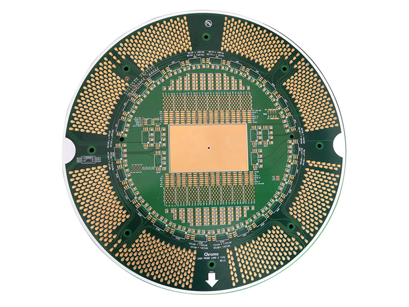
In Aug of 2020, we achieved HDI PCB used in the IC test.
This kind of board needs 50u” hard gold on pads, it’s 16 layers with FR-4 TG170 material, the blind & buried stack up is 1+1+12+1+1, min warp & twist is only 0.5%, copper is 1 OZ with min trace width/gap 3/3mil.
We also make some rigid-flex PCBs using in the same industry.
Eddi Yan
0755-26484826
0755-26484827
ECheng Industrial Park,Tongqiao Town,Zhongkai High-Tech Zone,Huizhou,Guangdong,China
Room 402-405, Fu Lin Building, Qiao Tou, Fu Yong, Baoan,Shenzhen,Guangdong,China