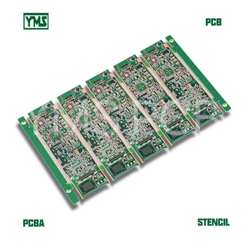
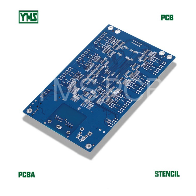
It has 4 layers board, we call 5G Cpe Pcb Circuit Board a multilayer PCB. Multilayer PCB is a circuit board that has more than two layers.
Unlike a Double-Sided PCB which only has two conductive layers of material, all multilayer PCBs must have at least three layers of conductive material that are buried in the center of the material.
Alternating layers of prepreg and core materials are laminated together under high temperature and pressure to produce Multilayer PCBs.
Pls contact us at [email protected] for your PCB/FPC/PCBA/FPCA/STENCIL/ASSEMBLY service.
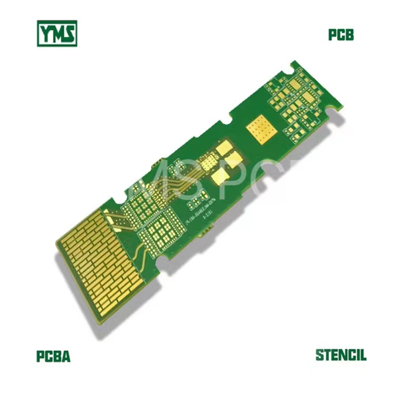
Part Number: 334-0 PCB
Layers: 4L PTFE
Board Thinkness:0.5mm
Base Material: Taconic TSM-DS3
Min Holes:0.3mm
Minimum Line Width/Clearance:0.2mm/0.2mm
Board Size:100mm x 50mm
Aspect Ratio:1.67: 1
Surface treatment: Immersion silver/Immersion Tin/Immersion Gold
Special point: Tight Etch Tolerances on Critical RF Features:+/- .0005″ standard tolerance for un-plated 0.5oz copper
Impedance: 50+5/-5Ω
Applications: Micro-wave
Minimum line width/gap:3.5/4mil (laser drill)
Minimum hole size:0.15mm (mechanical drill)/4mil (laser drill)
Minimum Annular Ring: 4mil
Max Copper thickness: 12OZ
Max Production size: 900×1200mm
Board Thickness: L2: 0.2-7.0mm, Multilayers:0.40-7.0mm,
Min Solder Mask Bridge:0.08mm
Aspect ratio: 20:1
Plugging Visa capability: 0.2-0.8mm, by resin or silver plug or copper plate to shut holes
Pls contact us at [email protected] for your PCB/FPC/PCBA/FPCA/STENCIL/ASSEMBLY service.
Eddi Yan
0755-26484826
0755-26484827
ECheng Industrial Park,Tongqiao Town,Zhongkai High-Tech Zone,Huizhou,Guangdong,China
Room 402-405, Fu Lin Building, Qiao Tou, Fu Yong, Baoan,Shenzhen,Guangdong,China