IC substrates serve as the connection between IC chip(s) and the PCB through a conductive network of traces and holes. IC substrates support critical functions including circuit support and protection, heat dissipation, and signal and power distribution.
IC substrates represent the highest level of miniaturization in PCB manufacturing and share many similarities with semiconductor manufacturing.
Pls contact us at [email protected] for your PCB/FPC/PCBA/FPCA/STENCIL/ASSEMBLY service.
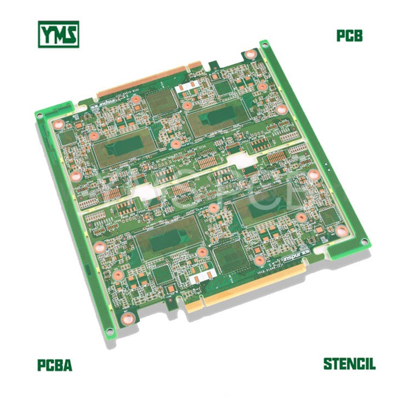
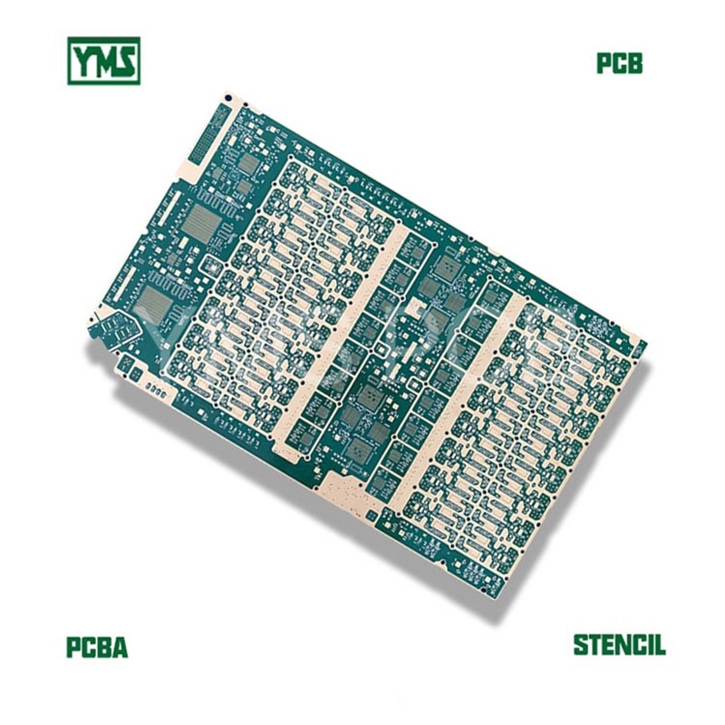
| Layer count | 8 |
| Material | FR-4 (M6 from PANANSONIC) |
| Board size(mm) | 164 X 256 |
| Board thickness | 1.8 mm |
| Layer copper | 1 OZ |
| Min through hole | 0.2mm(8mil) |
| Min trace width | 3mil(0.075mm) |
| Min trace gap | 3mil(0.075mm) |
| Surface treatment | Immersion Gold (ENIG) |
| Application | telecommunications and electronics hardware update |
| Solder mask color | Blue/green |
| Silkscreen | white |
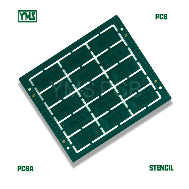
FC-CSP Features
High I/O Count and Short Interconnects
High layout density
Array type lead-free solder bump & Cu pillar bump
Build-up technology & Stack via
Fine Pattern formation
FC-CSP Specification
Package Size: 3 x 3 mm up to 15 x 15 mm
Line & Space: 15/15 um
Bump Pitch: down to 100 um
ETS, Coreless available
Application: Smartphones, Networks, PC, Servers, consumer electronics
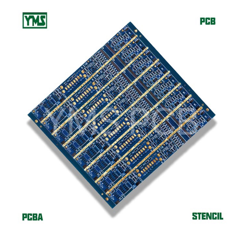
PBGA Features
High circuit density design
Good electrical performance
Good ability for heat dissipation
PBGA Specification
Package Size: 15x15mm up to 27x27mm
Line/Space: 20/20 um
Impedance control for critical signal traces
Application: DTV, Microprocessors/controller/ASICs, Infrastructure application.
Pls contact us at [email protected] for your PCB/FPC/PCBA/FPCA/STENCIL/ASSEMBLY service.
Eddi Yan
0755-26484826
0755-26484827
ECheng Industrial Park,Tongqiao Town,Zhongkai High-Tech Zone,Huizhou,Guangdong,China
Room 402-405, Fu Lin Building, Qiao Tou, Fu Yong, Baoan,Shenzhen,Guangdong,China