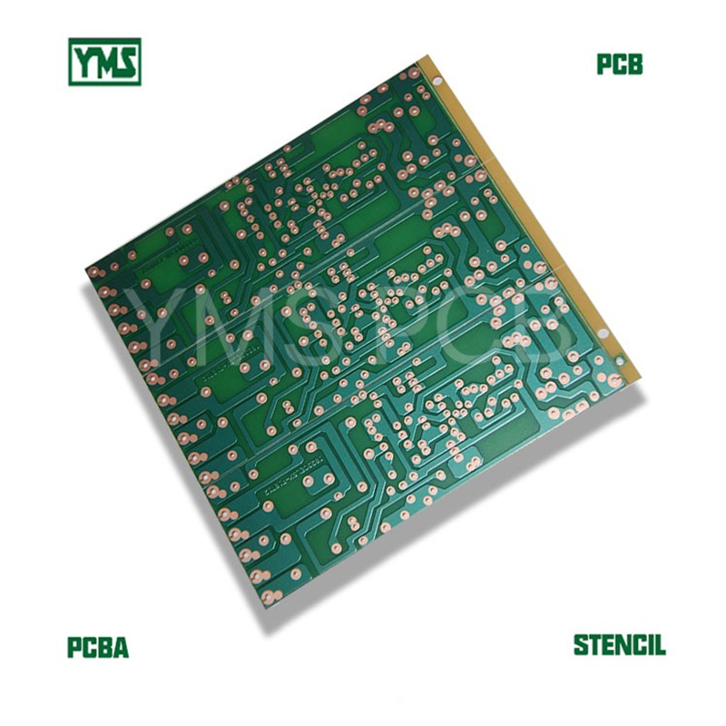
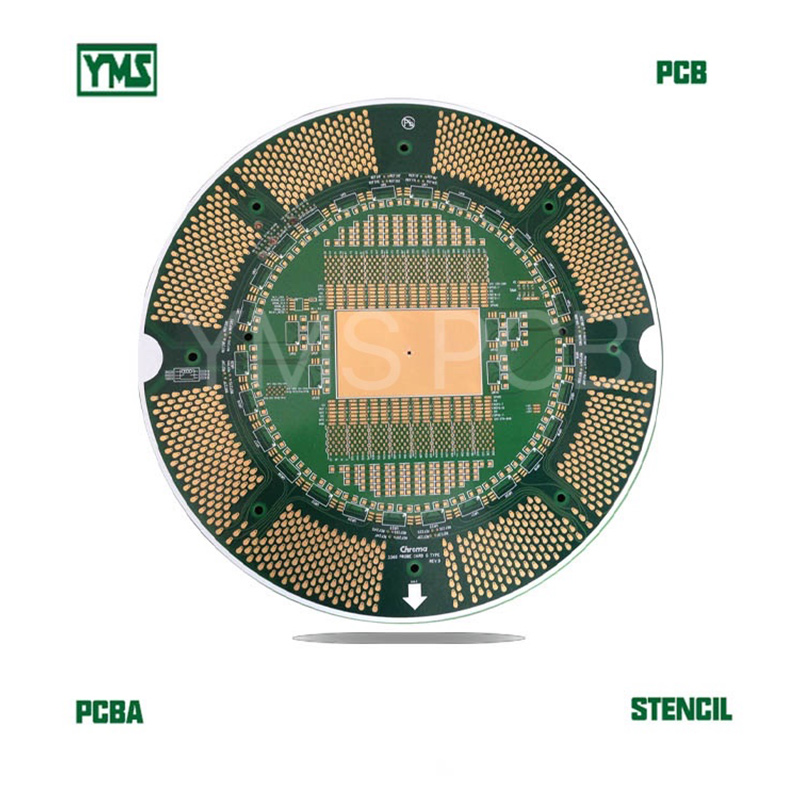
YMS PCB from Shenzhen China offer this 34 layers Printed Circuit Board, with the back drill and blind holes, back drill hole size is 0.5mm. The blind hole is 0.1mm drilled by laser machine, stack up is 1+32+1, 1 step HDI board. It’s used in semiconductor test equipment, so the min warp & twist is only 0.5%, much less than the IPC-II standard (0.75%). Board thickness is 5.0mm with 0.3mm holes, the aspect ratio is 17:1, need to do special control in PTH process.
Pls contact us at [email protected] for your PCB/FPC/PCBA/FPCA/STENCIL/ASSEMBLY service.
| Layer count | 34 |
| Material | FR-4 TG180 ITEQ(IT180A) |
| Board size(mm) | 350 X 350 |
| Board size(inch) | 13.78 X 13.78 |
| Board thickness | 5.0mm |
| Outer layer copper | 35um |
| Inner layer copper | 18um & 35um |
| Min hole | 0.3mm |
| Min trace width | 4mil(0.1mm) |
| Min trace gap | 4mil(0.1mm) |
| Surface treatment | Immersion gold (ENIG) |
| Aspect ratio | 17 : 1 |
| Application | semiconductor test equipment |
| Solder mask color | dark green |
| Silkscreen | white |
| Standard | IPC-II |
| Impedance | Yes |
min warp & twist is only 0.5% with big board size, and the copper weight is not the same for the inner layer, need to do special and high precision control when lamination. Our lamination equipment is from Germany with good quality.
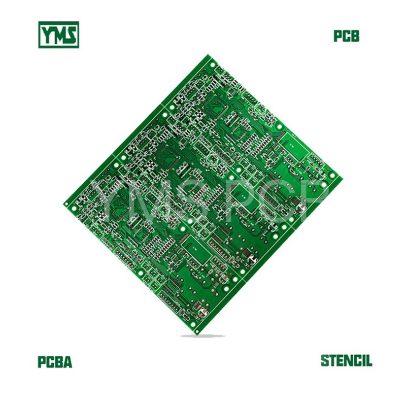
This board request the IPC-III standard, need to meet min 1mil(25um) at hole copper, the customer doesn’t accept repair on the circuit and solder mask.
Pls contact us at [email protected] for your PCB/FPC/PCBA/FPCA/STENCIL/ASSEMBLY service.
Eddi Yan
0755-26484826
0755-26484827
ECheng Industrial Park,Tongqiao Town,Zhongkai High-Tech Zone,Huizhou,Guangdong,China
Room 402-405, Fu Lin Building, Qiao Tou, Fu Yong, Baoan,Shenzhen,Guangdong,China