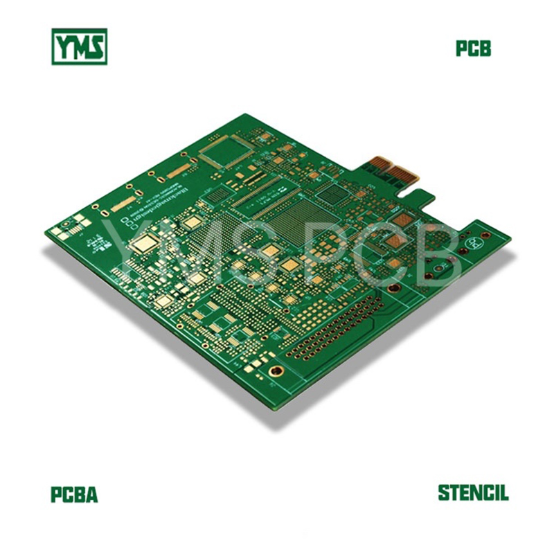
There are 3 difficult points for this 26-Layer Hdi Board printed circuit board:
1, high layer counts up to 26 layers—YMS can support 34 layers PCB.
2, HDI board with a laser drill, 2 step blind & buried holes with 3 times pressing.
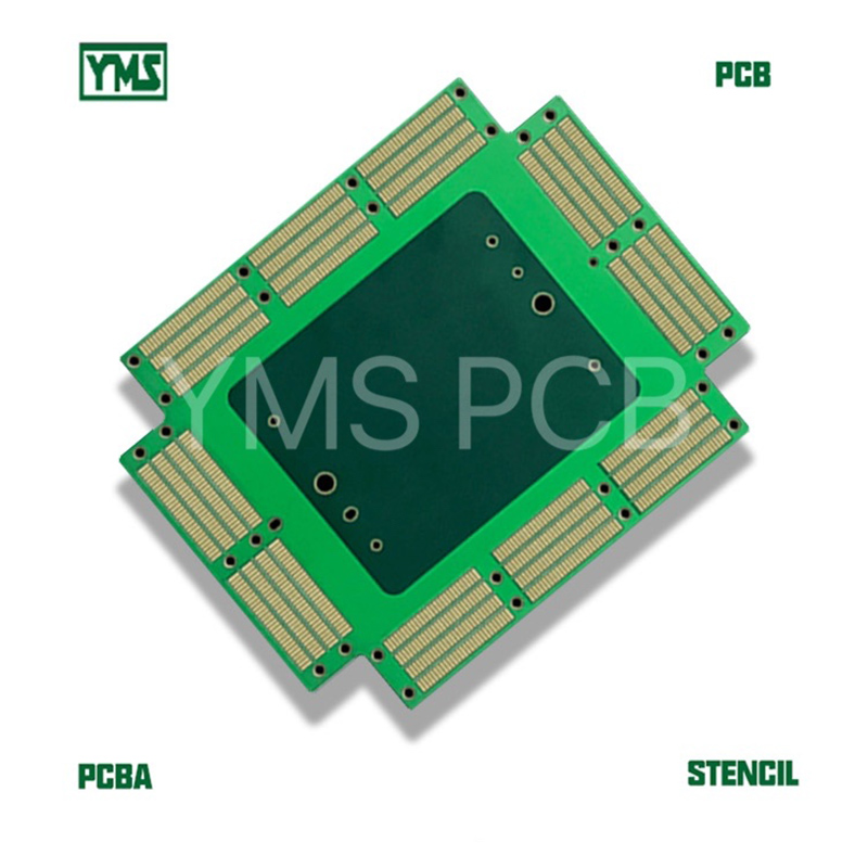
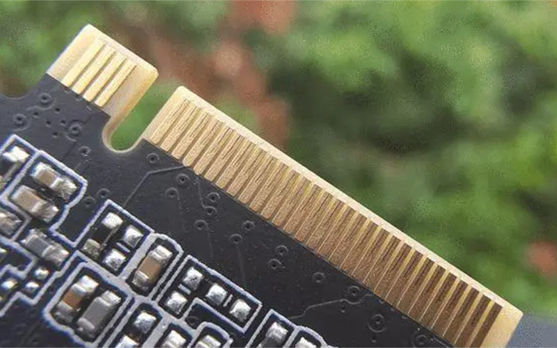
3, hard gold 200u” on gold fingers area, edge connector.
Pls contact us at [email protected] for your PCB/FPC/PCBA/FPCA/STENCIL/ASSEMBLY service.
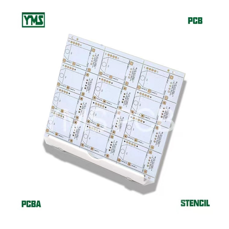
Layers: 26 layers with blind & buried holes and gold fingers
Board Thickness: 2.4mm+/-0.24mm
Copper weight: 1 OZ for the outer layer and H OZ for the inner layer
Material: FR-4 TG 180
Min Holes:0.2mm (8mil)
Minimum Line Width/Clearance:4mil/4mil
Board Size: 210mm x 121mm
Aspect Ratio: 12:1
Surface Treatment: ENIG (gold thickness 2u”) + gold fingers (edge connector) up to 200u”
Applications: telecom communication, aerospace, military
Impedance Control: yes
Back drill: yes, from bot side with 0.5mm holes
Resin plug holes: yes
Solder mask color: green
Silkscreen color: white
Normally the gold thickness on gold fingers (edge connectors) is 10-30u, but this product request 200u, it’s hard to control the gold thickness and quality because it’s too thick, but we do it well with our high precision equipment and professional management team.
Pls contact us at [email protected] for your PCB/FPC/PCBA/FPCA/STENCIL/ASSEMBLY service.
Eddi Yan
0755-26484826
0755-26484827
ECheng Industrial Park,Tongqiao Town,Zhongkai High-Tech Zone,Huizhou,Guangdong,China
Room 402-405, Fu Lin Building, Qiao Tou, Fu Yong, Baoan,Shenzhen,Guangdong,China