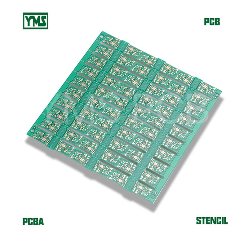
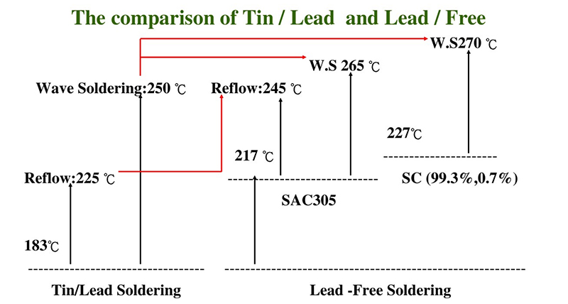
It’s a Lead-Free HAL board without lead and meets the RoHS compliant and REACH. YMS PCB offer a one-stop PCB (PRINTED CIRCUIT BOARD) solution since 2000, now we have over 21 years of experience with over 400 staff.
We support PCB design, BARE PCB fabrication, PCBA assembly, Component/Parts sourcing, STENCIL production. We support all kinds of PCB like RF Antenna PCBs, UAV PCBs, heavy, copper PCB up to 12 OZ, millimeter-wave radar PCB, high TG (TG170, TG180), ceramic PCB
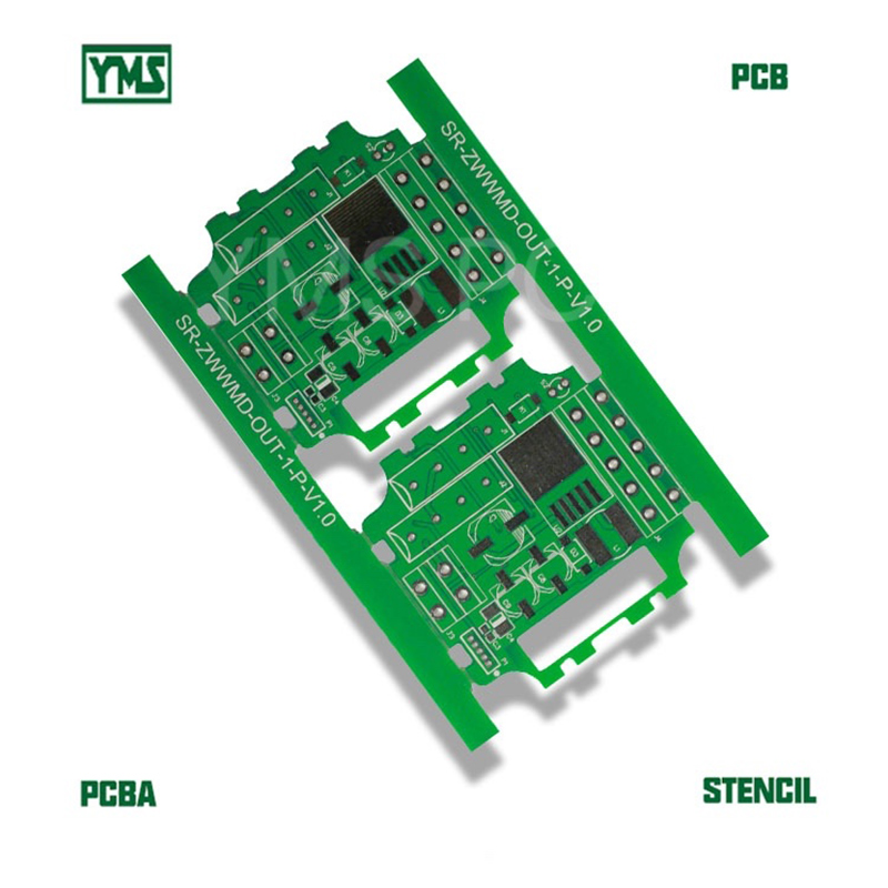
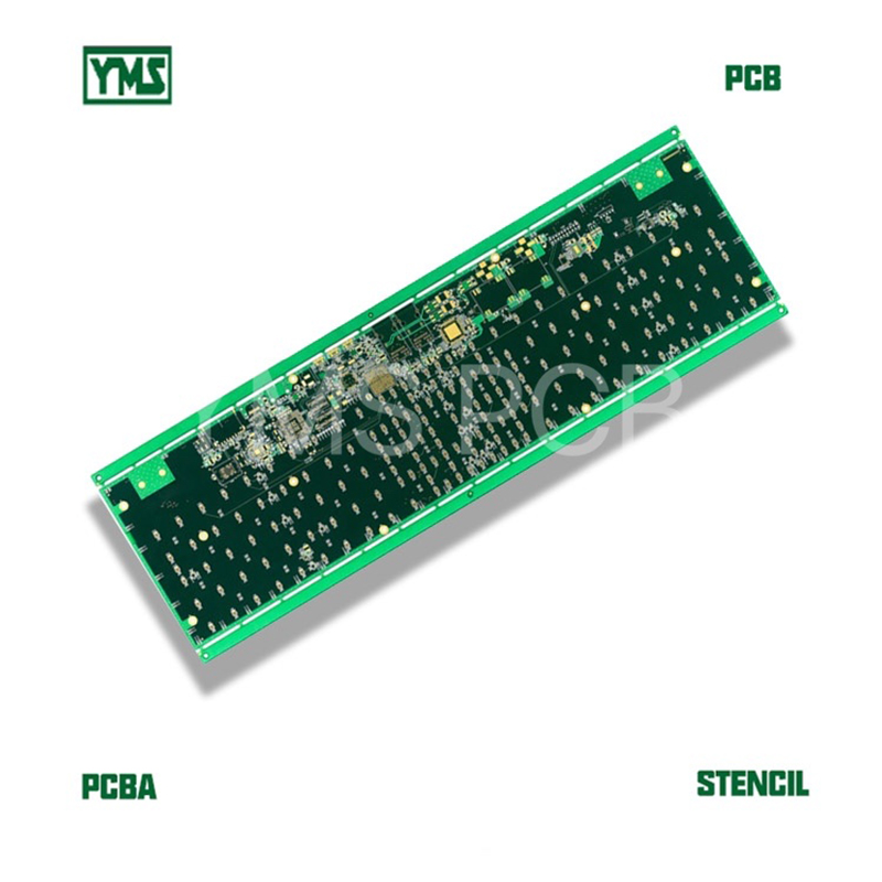
R and TS TF/RTS GK keyboard PCB.
Pls contact us at [email protected] for your PCB/FPC/PCBA/FPCA/STENCIL/ASSEMBLY service.
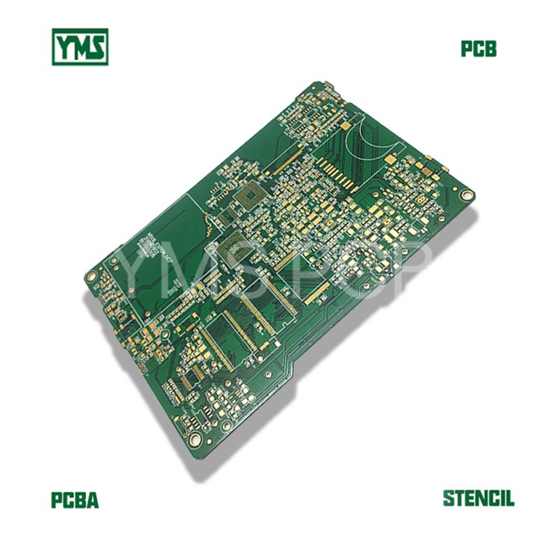
Layer count: 6 layers
Material: FR-4 TG150
Copper: 2/2/2/2/2/2 OZ (heavy copper for inner and outer layer)
Outline Tolerance: +/-0.15mm
Board size: 135 x 244.4 mm
Minimum line width / line distance: 0.1mm / 0.1mm (4mil/4mil)
Min hole: 0.15mm (6mil)
Thickness: 1.0mm ± 0.1mm
Surface treatment: Immersion Tin
Standard: IPC-II
Lead time: 3 days
Applications: Computer motherboard/daughterboard, Mobile Phone
This board request Immersion Tin, the Tin thickness is 1um
We support all kinds of PCB finish treatment like:
HAL (Leaded Hot Air Leveling)
LF HAL (Lead-Free Hot Air Leveling)
ENIG (Electroless Nickel/Immersion Gold)
Immersion Tin
Immersion Silver
OSP (Organic Solderability Preservatives)
Gold fingers (edge connector), from 10 to 200 u” gold thickness
Selective hard gold
Flash gold (gold plating)
Pls contact us at [email protected] for your PCB/FPC/PCBA/FPCA/STENCIL/ASSEMBLY service.
Eddi Yan
0755-26484826
0755-26484827
ECheng Industrial Park,Tongqiao Town,Zhongkai High-Tech Zone,Huizhou,Guangdong,China
Room 402-405, Fu Lin Building, Qiao Tou, Fu Yong, Baoan,Shenzhen,Guangdong,China