

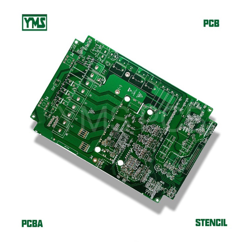

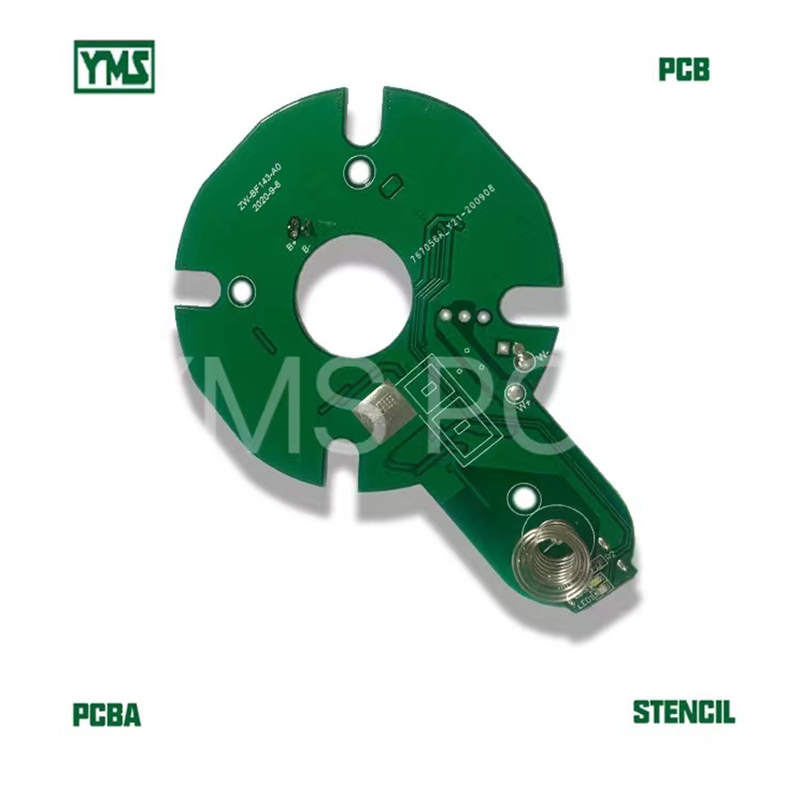
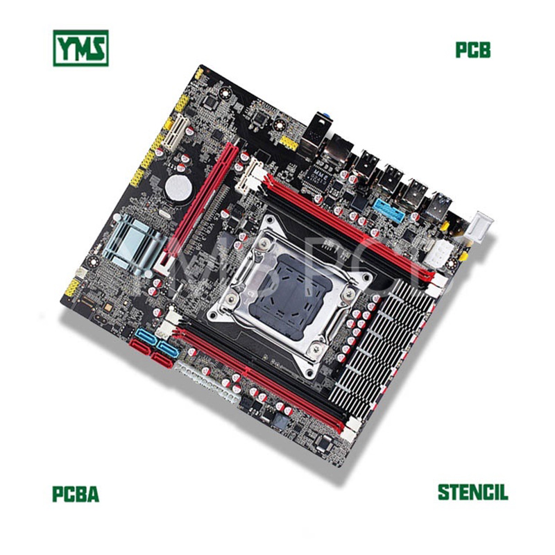
IC substrates serve as the connection between IC and the PCB (PRINTED CIRCUIT BOARD) by a conductive network between traces and holes. IC substrates represent the highest level of miniaturization in PCB manufacturing and share many similarities with semiconductor manufacturing.
YMS PCB focuses on IC substrates PCB and semiconductor PCB since 2012. IC substrate has been developing with the booming of new types of ICs like BGA and CSP which call for new carriers of package.
As one type of the most advanced PCB (Printed Circuit Board), IC substrate PCB has exploded in both popularity and applications together with any layer HDI PCB and flex-rigid PCB, now widely applied in telecommunications and electronics updates.
Pls contact us at [email protected] for your PCB/FPC/PCBA/FPCA/STENCIL/ASSEMBLY service.
| Layer count | 22 |
| Material | FR-4 TG180 ITEQ(IT180A) |
| Board size(mm) | 320 X 410 |
| Board size(inch) | 12.598 X 16.142 |
| Board thickness | 5.0mm |
| Outer layer copper | 30um |
| Inner layer copper | 18um & 35um |
| Min hole | 0.4mm |
| Min trace width | 4mil(0.1mm) |
| Min trace gap | 4mil(0.1mm) |
| Aspect ratio | 12.5:1 |
| Surface treatment | Immersion gold (ENIG) |
| Application | IC substrates, IC test PCB, semiconductor printed circuit board(PCB) |
| Solder mask color | black |
| Silkscreen | white |
| Standard | IPC-II |
| Impedance | Yes |
This is HDI board with laser holes, the blind and buried holes are on all layers.
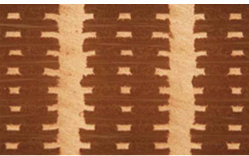
HDI PCB= High-Density Interconnect Printed Circuit Board, it’s widely used in the high technology industry like automotive, aerospace, telecom communication…also the products are widely used in IC substrate, IC test, semiconductor.
Pls contact us at [email protected] for your PCB/FPC/PCBA/FPCA/STENCIL/ASSEMBLY service.
Eddi Yan
0755-26484826
0755-26484827
ECheng Industrial Park,Tongqiao Town,Zhongkai High-Tech Zone,Huizhou,Guangdong,China
Room 402-405, Fu Lin Building, Qiao Tou, Fu Yong, Baoan,Shenzhen,Guangdong,China
