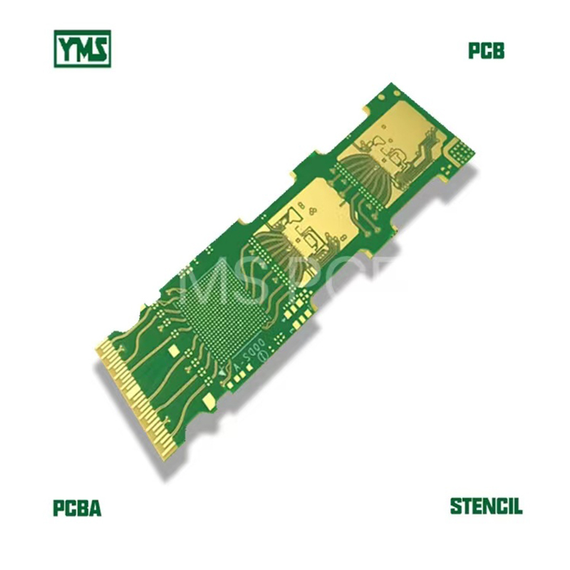
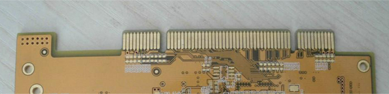
The PCB (PRINTED CIRCUIT BOARD) has a selective hard gold area, which means “50u” hard gold on the request pads and ENIG for other pads. The Hard Gold surface finish, also known as Hard Electrolytic Gold, is composed of a layer of gold with added hardeners for increased durability, plated over a barrier coat of nickel using an electrolytic process.
Hard gold is extremely durable, so during PCB Fabrication, this finish is usually applied to high-wear areas, such as edge connector Gold Fingers and keypads, since the hardness of the finish can withstand repeated use; however, due to the high cost of hard gold, and its relatively poor solder-ability, it is very rarely applied to solder-able areas.
Pls contact us at [email protected] for your PCB/FPC/PCBA/FPCA/STENCIL/ASSEMBLY service.
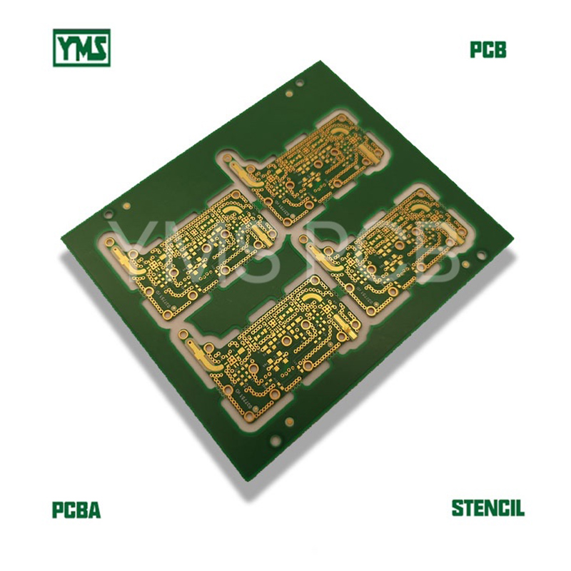
Layers: 8 layers
Board Thickness: 1.0mm+/-0.1mm
Copper weight: 1 OZ for outer layer & inner layer
Material: FR-4 TG 140
Min Holes: 0.2mm (8mil)
Minimum Line Width/Clearance: 0.13mm/0.15mm (5mil/6mil)
Board Size: 160mm x 100mm (0.63 x 3.937 inch)
Surface Treatment: ENIG (gold thickness 2u”) + gold fingers with selective hard gold “50u”
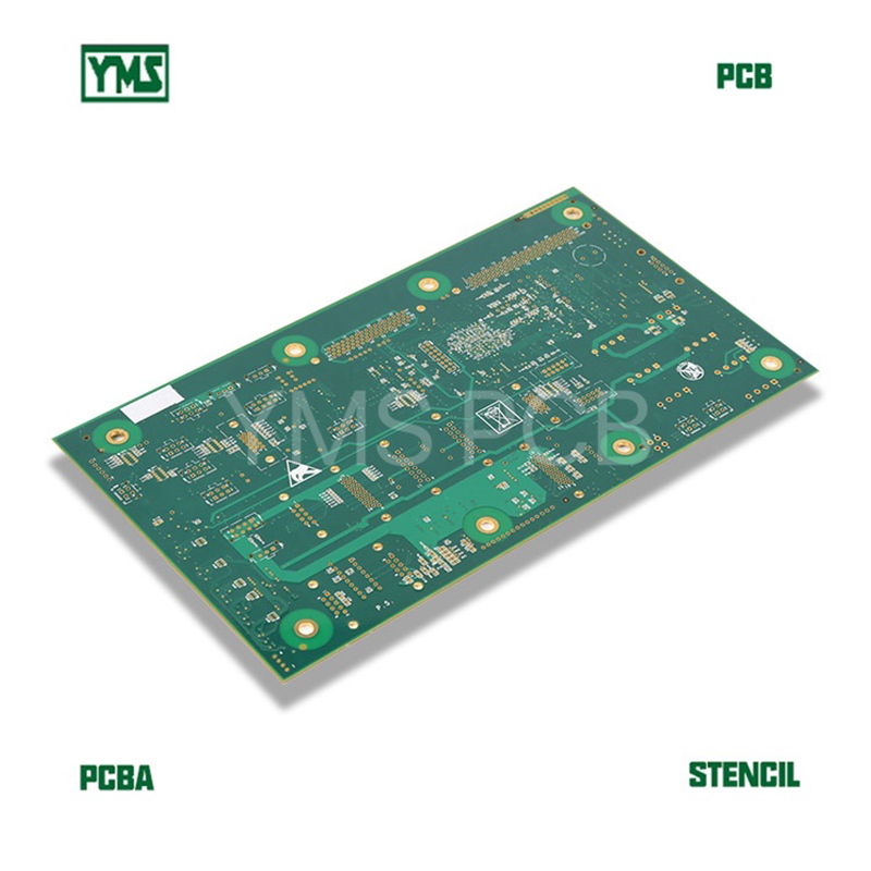
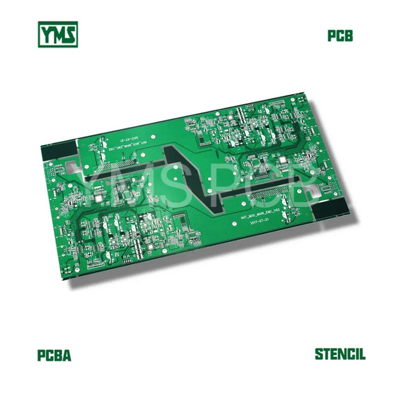
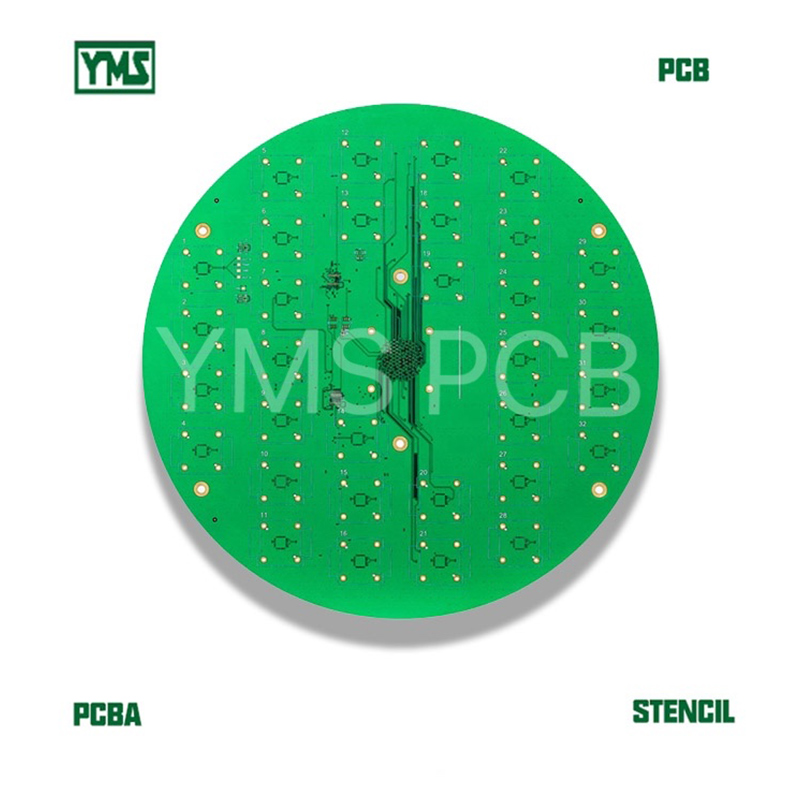
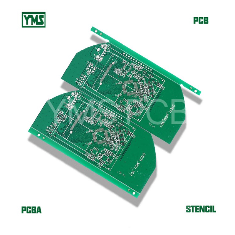
Applications: auto PCB/intelligent PCB/Communication PCB
Computer PCB/Security PCB/Industrial control PCB/LED PCB/Power supply PCB/Medical PCB
Impedance Control: Yes
Solder mask color: green/yellow/black with matt
Silkscreen color: white/yellow
There are conventional PCB printed circuit boards, with “50u” hard gold on edge connectors (gold fingers), we build the conductor circuit patterns on copper cladding laminates and electrical connections are formed between layers via holes.
After long-term development, the process technology has developed from single-sided up to 40 layers. YMS PCB mainly produces 1~34 layers multilayer PCB, with a maximum copper thickness of 12OZ for the outer layer and 8 OZ for the inner layer. The surface finish includes Lead-free HASL, ENIG, immersion silver, immersion tin, OSP, ENEPIG, gold fingers, etc.
Pls contact us at [email protected] for your PCB/FPC/PCBA/FPCA/STENCIL/ASSEMBLY service.
Eddi Yan
0755-26484826
0755-26484827
ECheng Industrial Park,Tongqiao Town,Zhongkai High-Tech Zone,Huizhou,Guangdong,China
Room 402-405, Fu Lin Building, Qiao Tou, Fu Yong, Baoan,Shenzhen,Guangdong,China