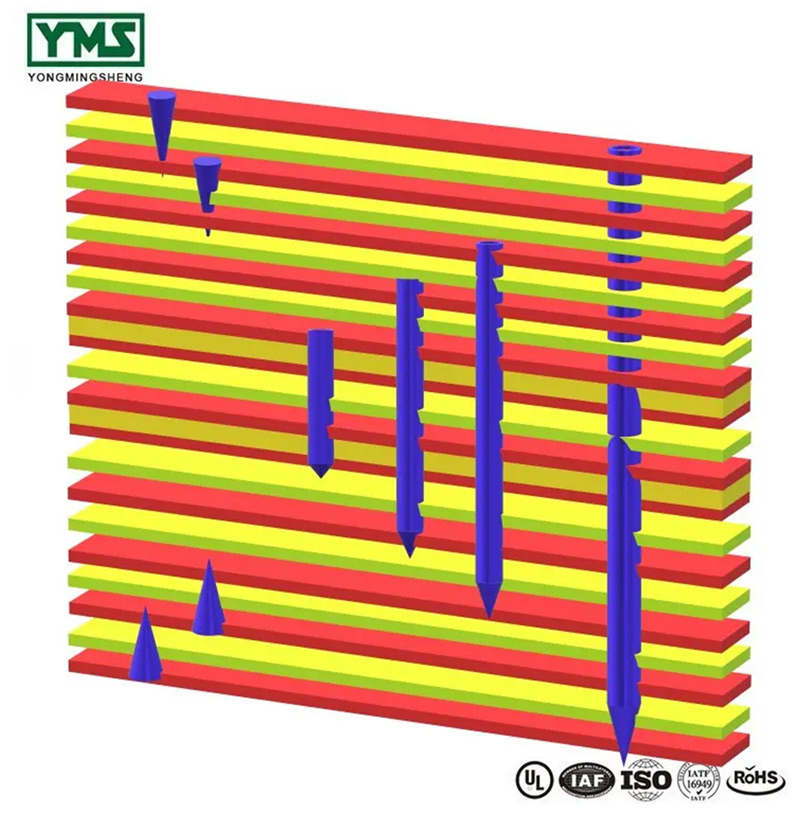
HDI= High-Density Interconnect, PCB=Printed Circuit Board
HDI PCB includes small trace width and space (maybe 3/3mil or smaller), small through holes (maybe 0.15mm or smaller), and very small BGA pads like 8mil, 10mil.
Pls contact us at [email protected] for your PCB/FPC/PCBA/FPCA/STENCIL/ASSEMBLY service.
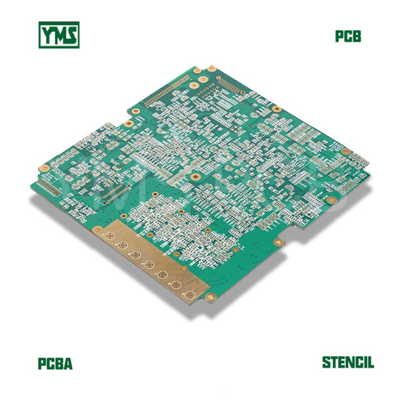
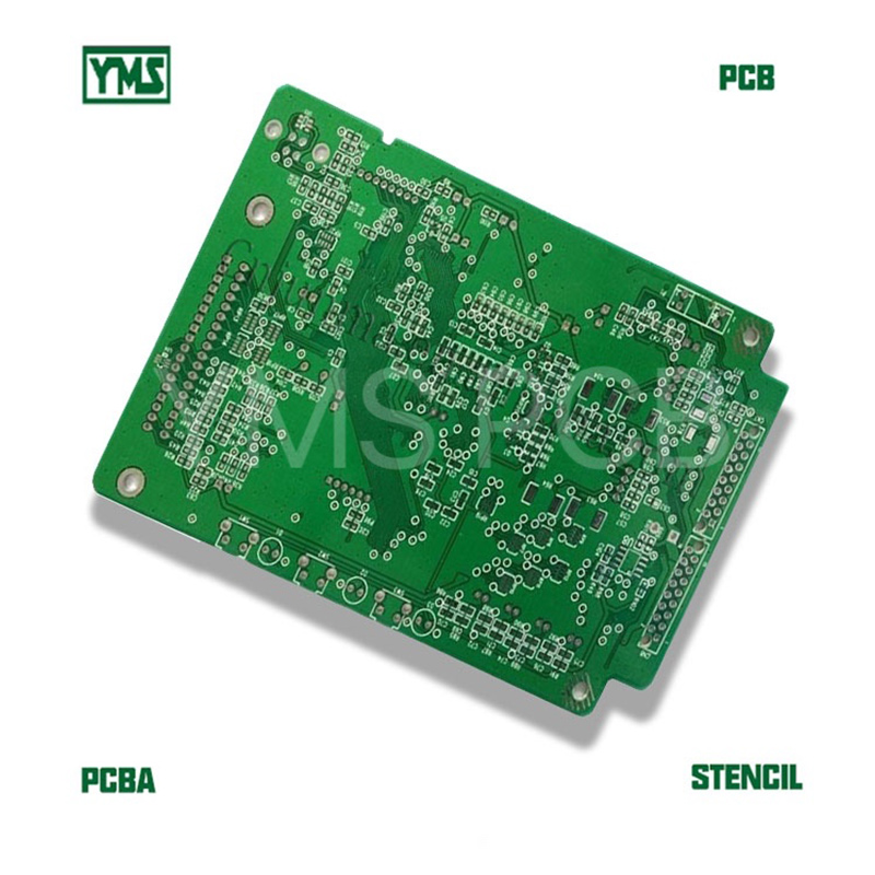
| Layer count | 12 |
| Material | FR-4 TG80 |
| Board size(mm) | 145 X 132 |
| Board thickness | 2.2 mm |
| Layer copper | 1/1/1/1/1/1/1/1/1/1/1/1 OZ |
| Blind & buried holes stack up | L1-L2, L2-L3, L3-L10, L4-L9, L5-L8, L10-L11, L11-L12 |
| Aspect Ratio: | 8:1 |
| Min hole | 0.1 mm by laser |
| Min trace width | 3mil |
| Min trace gap | 4mil |
| Surface treatment | ENIG |
| Application | Automotive |
| Solder mask color | green |
| Silkscreen | white |
| Standard | IPC-II |
| Impedance | YES |
HDI PCBs have blind & buried holes, usually contain micropores with a diameter of 0.006 or smaller.
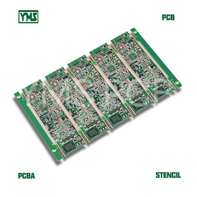
HDI PCB, Printed Circuit Boards offer the finest trace structures, with micro-vias drilled by laser machine.
HDI technology enables a highly compact, reliable printed circuit board design.
Also applied are Via-in-Pad and multiple micro-via-layers.
The most common reason for using HDI technology is a significant increase in packaging density.
YMS PCB Support All Kind Of HDI PCB With Stack Up As Below
1+N+1
2+N+2
3+N+3
4+N+4
5+N+5
Any Layers And Connection
Pls contact us at [email protected] for your PCB/FPC/PCBA/FPCA/STENCIL/ASSEMBLY service.
Eddi Yan
0755-26484826
0755-26484827
ECheng Industrial Park,Tongqiao Town,Zhongkai High-Tech Zone,Huizhou,Guangdong,China
Room 402-405, Fu Lin Building, Qiao Tou, Fu Yong, Baoan,Shenzhen,Guangdong,China