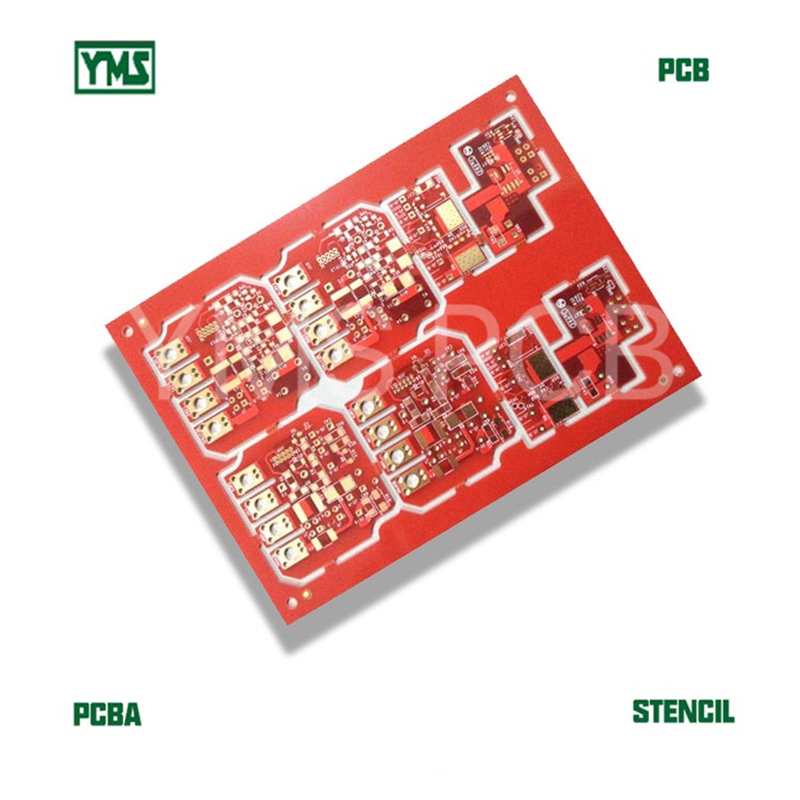
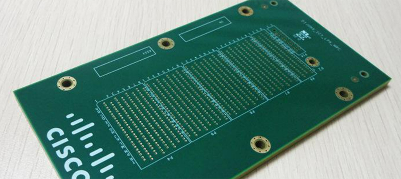
Telecom Communication PCB is a very high-precision product, it’s a specialized nature of the PRINTED CIRCUIT BOARD. Normally it’s backplane PCB, back thicker than conventional PCB board and heavy, and accordingly, its heat capacity is also large.
Backplane PCB generally refers to larger format printed circuit boards that are used as backbones for connecting several PCBs to ultimately form a computer bus.
Pls contact us at [email protected] for your PCB/FPC/PCBA/FPCA/STENCIL/ASSEMBLY service.
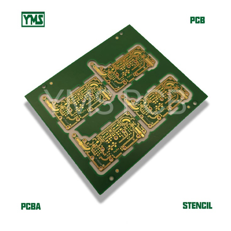
| Layer count | 5 |
| Material | FR-4 TG170 |
| Board size(mm) | 154 X 217 |
| Board size(inch) | 6.063 X 8.543 |
| Board thickness | 5.2 mm |
| Outer layer copper | 35um |
| Inner layer copper | 35um |
| Min hole | 0.4mm |
| Min trace width | 7mil |
| Min trace gap | 4mil |
| Blind & buried holes Stack up: | L1-L2, L2-L3, L1-L3, L3-L4 |
| Surface treatment | ENIG |
| Application | Telcom communication |
| Solder mask color | green |
| Silkscreen | white |
| Special point | 30um hole copper with HDI laser holes |
| Impedance | Yes |
This is a 5-layer board using in the telecom communication industry, with HDI laser holes.
Laser hole is from L1-L2, L2-L3, L1-L3, L3-L4.
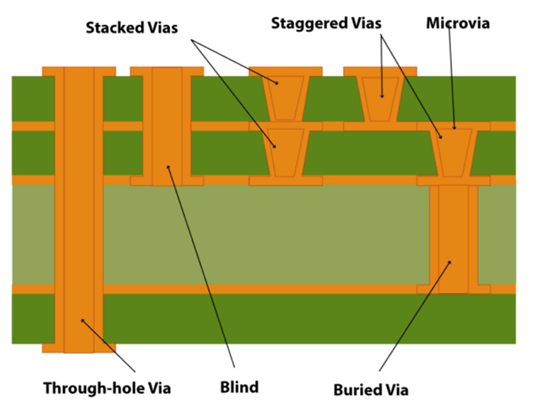
The hole copper of this board request 30um which is thick and need to do extra hole plating—hole copper is 20um in IPC-II, hole copper is 25um in IPC-II, so this PCB request higher hole copper than IPC-III.
Pls contact us at [email protected] for your PCB/FPC/PCBA/FPCA/STENCIL/ASSEMBLY service.
Eddi Yan
0755-26484826
0755-26484827
ECheng Industrial Park,Tongqiao Town,Zhongkai High-Tech Zone,Huizhou,Guangdong,China
Room 402-405, Fu Lin Building, Qiao Tou, Fu Yong, Baoan,Shenzhen,Guangdong,China