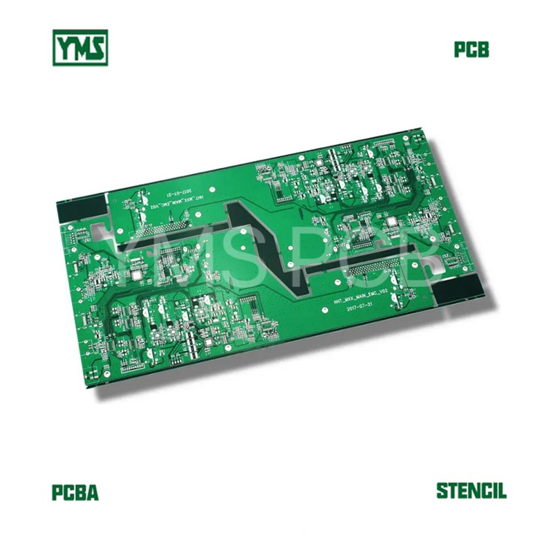
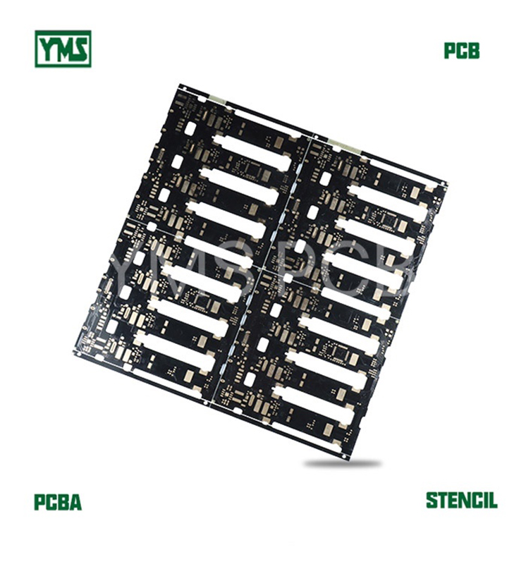
It’s 30 layers HDI board with small BGA pads, the BGA is only 10mil with 4mil laser holes on it.
The BGA vias are plugged by non-conductive (resin) then plating over and copper capped.
VIA-IN-HOLE process is very popular in our plant.
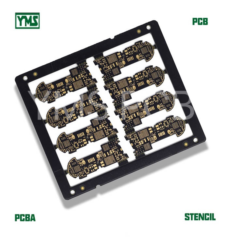
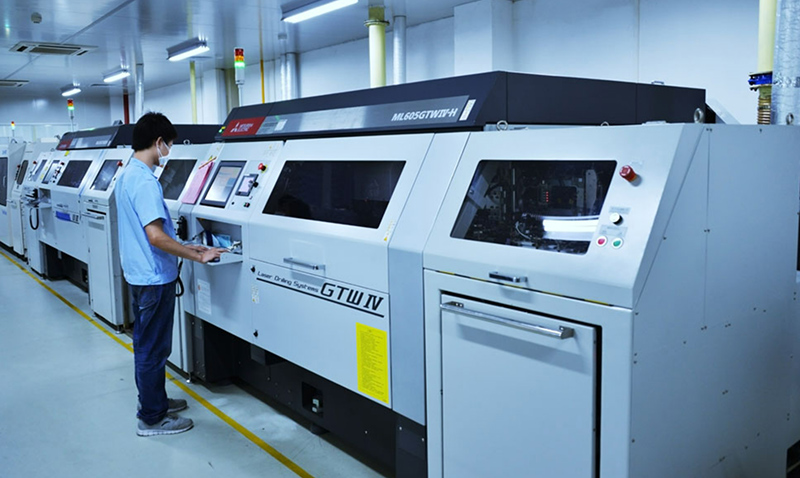
We Have Our Laser Drill Machine Inside To Ensure High Quality And On-Time Delivery. We can finish the HDI board in 5-7 days for quick-turn service.
Pls contact us at [email protected] for your PCB/FPC/PCBA/FPCA/STENCIL/ASSEMBLY service.
| Layer count | 30 |
| Material | FR-4 TG180 (IT-180A, ITEQ) |
| Board size(mm) | 64 X 56 |
| Board size(inch) | 2.52 X 2.205 |
| Board thickness | 2.0 mm (80mil) |
| Stack up: | 1+1+1+24+1+1+1 |
| Layer copper | Outer layer 1 OZ, inner layer 1OZ & HOZ |
| Min through hole | 0.2mm(8mil) |
| Min laser hole | 0.1mm(4mil) |
| Min trace width | 3mil(0.075mm) |
| Min trace gap | 3mil(0.075mm) |
| Surface treatment | Immersion Gold (ENIG) |
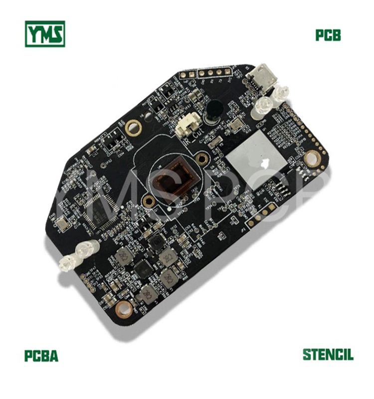
| Application | Mobile phone, telecom communication |
| Solder mask color | black |
| Silkscreen | white |
| Standard | IPC-II |
| Impedance | YES |
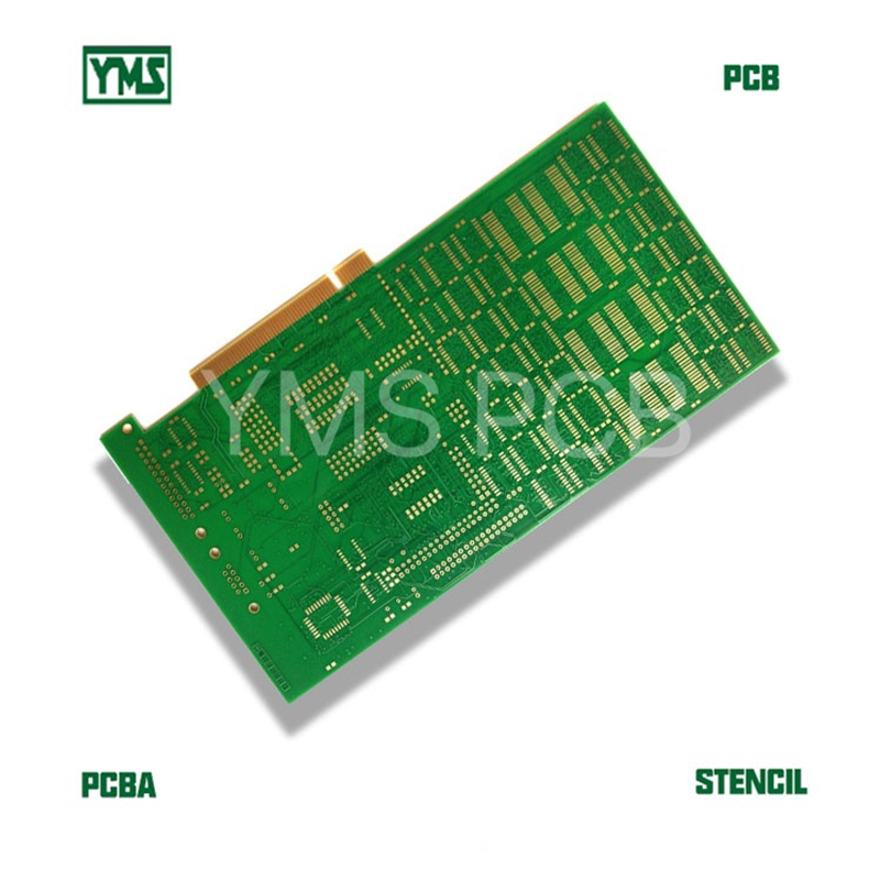
This HDI PCB (circuit board) is made by raw material IT-180A from ITEQ, it’s stable HIGH TG material. It’s made through multiple laser drilling and compression bonding. HDI PCB with blind & buried laser holes is widely used in high-end smartphones and other fields.
Pls contact us at [email protected] for your PCB/FPC/PCBA/FPCA/STENCIL/ASSEMBLY service.
Eddi Yan
0755-26484826
0755-26484827
ECheng Industrial Park,Tongqiao Town,Zhongkai High-Tech Zone,Huizhou,Guangdong,China
Room 402-405, Fu Lin Building, Qiao Tou, Fu Yong, Baoan,Shenzhen,Guangdong,China