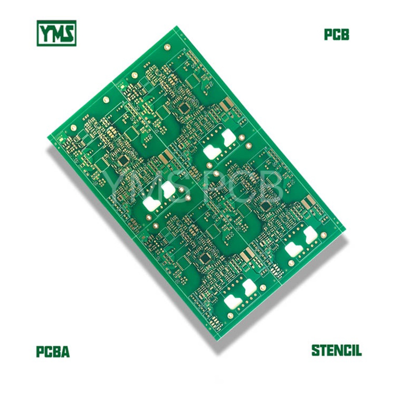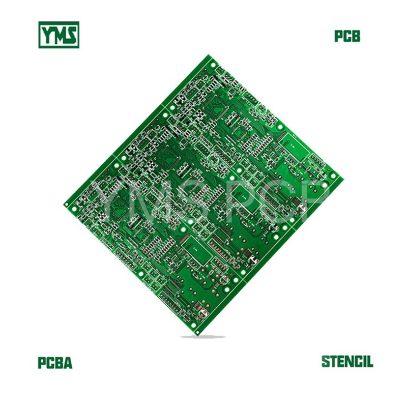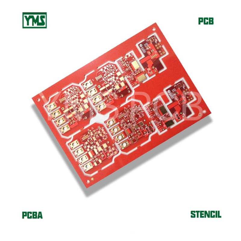
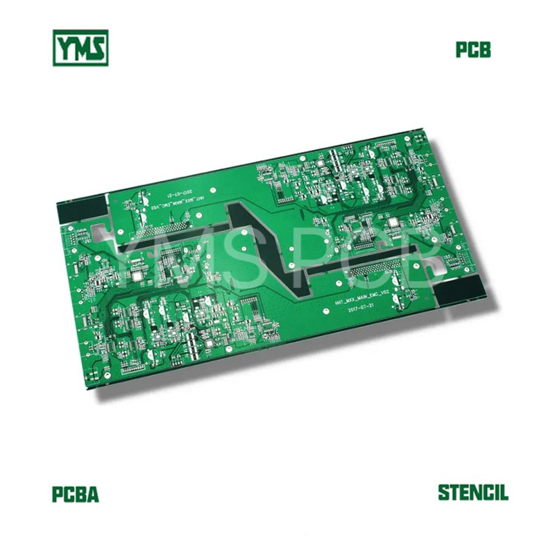
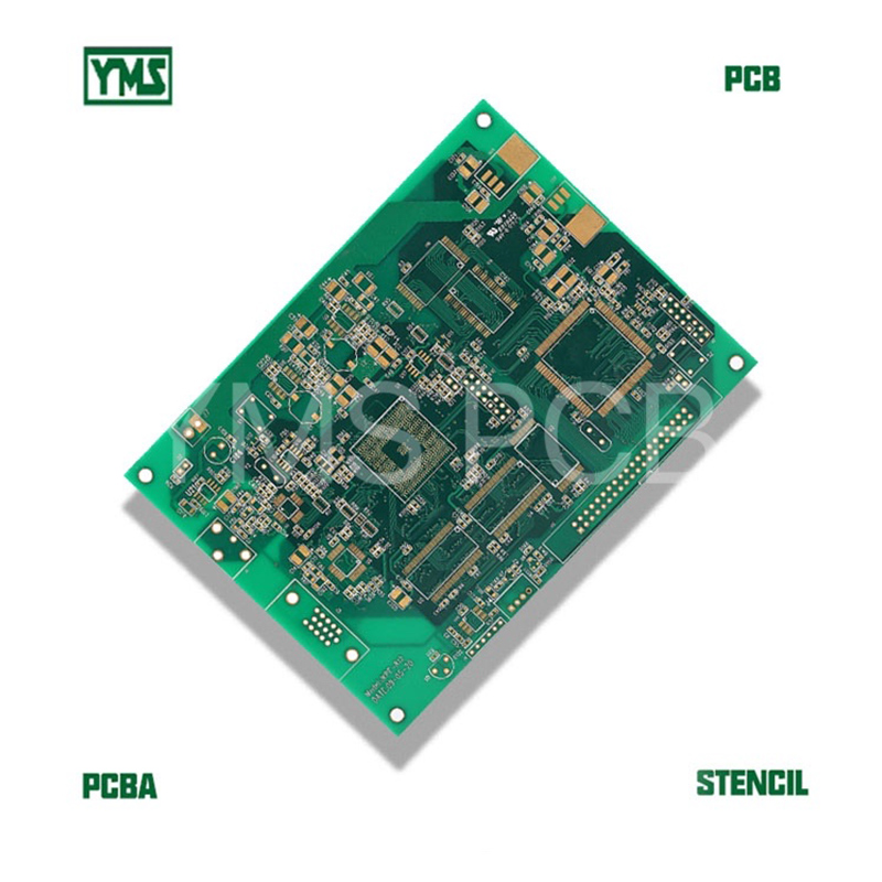
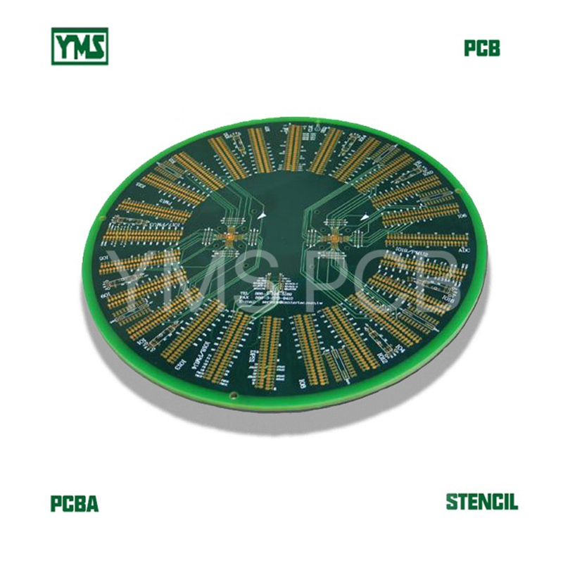
This special PCB is used in semiconductor test products, the min warp & twist is only 0.5%, the flatness of the PCB is very important to this product. Most of these products are HDI boards.
HDI–High-Density Interconnect PCB–Printed Circuit Board are defined as PCBs with higher wiring density per unit area than conventional PCBs. Nowadays, HDI PCBs are increasingly being used, and have made a big difference to technological advancement in the electronics industry.
Pls contact us at [email protected] for your PCB/FPC/PCBA/FPCA/STENCIL/ASSEMBLY service.
| Layer count | 16 |
| Material | FR-4 High TG, TG170, TG150, TG180 |
| Board size(mm) | 251 X 251 |
| Board thickness | 4.5mm |
| Outer layer copper | 1 OZ |
| Inner layer copper | 1 OZ |
| Min hole | 0.3mm |
| Min trace width | 3.5mil |
| Min trace gap | 3.5mil |
| Aspect ratio | 15:1 |
| Surface treatment | Flash plating gold, selective hard gold |
| Application | The semiconductor industry, telecom communication, military industry |
| Solder mask color | Green/blue/white/red/yellow/orange/purple |
| Silkscreen | White/yellow/black |
| Standard | MIL |
| Impedance | Yes |
We support all kinds of PCB, includes HF(High-Frequency) & RF (Radio Frequency) board, Impedance controlled board, HDI board, BGA& Fine Pitch board. The benefits explained above make these PCBs suitable for use in several applications, which include Medical Equipment, Industrial Control, Aerospace, consumer products, and Military.
Pls contact us at [email protected] for your PCB/FPC/PCBA/FPCA/STENCIL/ASSEMBLY service.
Eddi Yan
0755-26484826
0755-26484827
ECheng Industrial Park,Tongqiao Town,Zhongkai High-Tech Zone,Huizhou,Guangdong,China
Room 402-405, Fu Lin Building, Qiao Tou, Fu Yong, Baoan,Shenzhen,Guangdong,China