

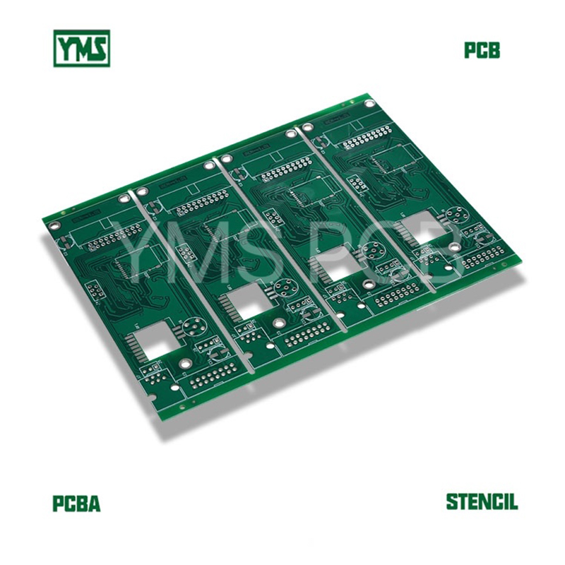

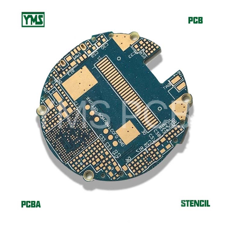
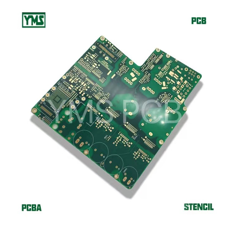
There are special technical points of this PCB—PRINTED CIRCUIT BOARD
1. There are back drill holes from the bot side, it’s a new technology in the PCB industry, and whole size is 0.5mm. This is 10 layers board with 2.0mm thickness, the back drill holes are drilled from both sides with depth control to 1.0+/-0.1mm, the same as the blind hole but with new technology.
2. There is a peelable mask on the bot side, also called a blue mask. We use PETERS for the peelable masks. The peelable mask is protecting the holes which don’t need to do the assembly in the SMT process, then can peel it off by hand when necessary after SMT and do DIP.
Pls contact us at [email protected] for your PCB/FPC/PCBA/FPCA/STENCIL/ASSEMBLY service.
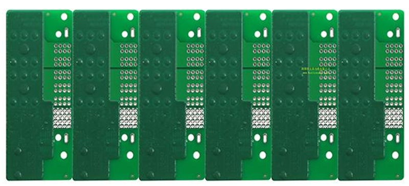
| Layer count | 10 |
| Material | FR-4 TG150 |
| Board size(mm) | 265.12 X 153.23 |
| Board thickness | 2.0 mm |
| Layer copper | 1 OZ for outer layer and H OZ for inner layer |
| Min through hole | 0.2mm(8mil) with 0.5mm back drill |
| Min trace width | 4mil(0.1mm) |
| Min trace gap | 4mil(0.1mm) |
| Surface treatment | Immersion Gold + OSP + Peelable mask |
| Application | Computer, consumer product |
| Solder mask color | Blue/green |
| Silkscreen | white |
Most of the back drill board is backplane board. Backplane PCBs often incorporate a wide variety of features including blind / buried vias, high-speed PCB/ high-speed materials, back drilling, counter bore, high aspect ratio and controlled impedance.
Backplane PCB usually used a Printed Circuit Board also have been used in minicomputers and high reliability applications.
Pls contact us at [email protected] for your PCB/FPC/PCBA/FPCA/STENCIL/ASSEMBLY service.
Eddi Yan
0755-26484826
0755-26484827
ECheng Industrial Park,Tongqiao Town,Zhongkai High-Tech Zone,Huizhou,Guangdong,China
Room 402-405, Fu Lin Building, Qiao Tou, Fu Yong, Baoan,Shenzhen,Guangdong,China
